Photonic and Quantum Materials
Tystar Corporation specializes in advanced semiconductor processing equipment, including low-pressure chemical vapor deposition (LPCVD) furnaces and photo-enhanced CVD systems. Their unique offerings—crack-free optical-grade silicon nitride (Si3N4) films up to 3 µm, thick optical-grade silicon oxide (SiO2) layers up to 30 µm via oxidation, and low-temperature (80 – 250 °C) defect-free deposition of nitrides and oxides—align closely with the demands of emerging photonic integrated circuits (PICs) and quantum computing technologies. These processes enable high-performance, low-loss materials essential for manipulating light at the nanoscale, reducing propagation losses, and integrating sensitive quantum components without thermal damage. Below, we explore their applications with specific examples, focusing on how Tystar’s advantages mitigate key challenges in these fields.
1. Hydrogen-Free 3 µm Crack-Free Si3N4 LPCVD
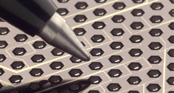
Silicon nitride (Si3N4) is a foundational material for high-performance photonics and quantum systems due to its ultra-low optical loss, wide transparency window (from visible to mid-infrared), and high optical power handling capacity. The primary challenge for using thick Si3N4 films (>600 nm for strong optical confinement) is the high tensile stress in LPCVD films, which causes cracking or delamination. Tystar’s capability to deposit up to 3 µm of high-quality, hydrogen-free Si3N4 without defects overcomes these stress limitations, enabling ultra-low-loss waveguides in PICs, as Si3N4 offers broadband transparency and minimal absorption in visible to near-infrared wavelengths. This supports mass manufacturing of dense PICs for telecommunications and datacom, where thick, uniform films ensure reliability.
2. Record-Setting 30 µm SiO2 Oxidation
Silicon dioxide (SiO2) serves as the primary cladding and buffer layer in silicon-based photonics, isolating the high-index core (e.g., Si or Si3N4) from the substrate. To prevent light leakage (evanescent coupling) into the substrate, especially in mid-infrared or high-power applications, a very thick, high-uniformity oxide layer is necessary. Tystar’s thick optical-grade SiO2 oxidation, achieving a world record setting at 30 µm, provides superior cladding for waveguides, isolating light paths and minimizing crosstalk in silicon photonics platforms. This is crucial for hybrid silicon-silicon nitride platforms, enhancing functionalities like optical signal processing. Notably, researchers at Caltech have leveraged Tystar’s SiO2 oxidation capabilities to achieve world record quality factors (Q ∼ 109) in optical resonators, as reported in Nature Photonics[1].
3. Low-Temp (80 – 250 °C) Photo-Enhanced CVD
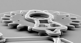
The development of heterogeneous integrated circuits, where photonic or quantum devices are combined with pre-fabricated electronics (e.g., CMOS), requires low-temperature deposition processes to avoid damaging the underlying metallization or active components. Tystar’s PhotoEnhanced CVD uses UV light to activate process gases, eliminating the need for high-temperature plasma, which causes ion-induced radiation damage. This low-temperature photo-enhanced CVD (80 – 250 °C) allows void-free deposition of nitrides and oxides on temperature-sensitive substrates, enabling integration with III-V materials or polymers. This facilitates flexible PICs for biophotonics, such as wearable sensors, where low-heat processes preserve substrate integrity.
Table 1: Applications of Thick Si3N4 LPCVD
| Application | Tystar Advantage | Specific Examples |
|---|---|---|
| High-Confinement Waveguides | Mitigation of Film Stress and Cracking: The ability to deposit up to 3 µm of highquality Si3N4 without defects overcomes stress-limitations that constrain other fabrication platforms. | Ultra-Low Loss Si3N4 Waveguides (e.g., 4 µm × 1 µm cross-sections) for long-distance on-chip signal routing with near-fiber-like propagation loss (<0.1 dB·cm-1), critical for large-scale PICs and quantum networks. In LiDAR systems for autonomous vehicles, this enables low-loss optical beamforming networks, improving range and resolution. |
| Integrated Nonlinear Optics | High Power Handling and Enhanced χ(3) Nonlinearity: Thicker films enable stronger optical confinement, which, combined with Si3N4’s high Kerr nonlinearity (χ(3)), is essential for high-efficiency frequency conversion. | Kerr Frequency Comb Generators for optical clocks and massive data transmission. The highquality Si3N4 is used to fabricate ultra-high-Q microresonators that produce highly coherent optical frequency combs. In frequency comb-based quantum processors, crack-free Si3N4 waveguides enable scalable multi-qubit operations at room temperature. |
| Photonic Quantum Sources | Low Material Loss for Coherence: Minimizing optical loss is paramount for maintaining quantum coherence and entanglement. | Integrated Single-Photon Sources and Beam Splitters built from low-loss waveguides, enabling complex quantum algorithms and quantum entanglement generation on a single chip. In photonic quantum computing, Si3N4 films support quantum photonic integrated circuits (QPICs) for generating and routing entangled photons with ultra-low losses. |
4. Summary
Tystar’s cutting-edge technologies are poised to transform industries by enabling next-generation photonic and quantum computing solutions. Their ability to create high-quality, thick silicon nitride films without defects powers faster, more reliable data transmission in devices like LiDAR for self-driving cars and quantum networks for secure communication. Their world-record silicon oxide layers enhance stability and performance in advanced sensors and quantum processors, critical for applications in healthcare and computing. Additionally, Tystar’s low-temperature deposition process allows integration with sensitive materials, opening doors to innovative products like wearable health monitors and compact data center transceivers. By addressing key manufacturing challenges, Tystar’s solutions drive scalability and cost-efficiency, positioning the company as a leader in the rapidly growing markets of photonics and quantum technology, with applications spanning telecommunications, autonomous vehicles, and secure computing.
Table 2: Applications of Record-Setting SiO2 Oxidation
| Application | Tystar Advantage | Specific Examples |
|---|---|---|
| High-Q Optical Resonators | Maximum Substrate Isolation and Uniformity: Growing thermal oxide up to 30 µm ensures perfect isolation of the optical mode, reducing leakage loss and improving resonator quality factor (Q). Tystar’s demonstrated capability has enabled world-record Q-values (up to ∼ 109 ). | High-Q Optical Microdisk and Microsphere Resonators used as compact, stable reference lasers or as high-finesse cavities for cavity quantum electrodynamics (cQED) experiments, boosting light-matter interaction. In spectrometers for life sciences, thick oxide layers support high-resolution on-chip sensors. |
| Thermal and Mechanical Isolation | Exceptional Cladding and Buffer Properties: The thick, high-density thermal oxide provides superior mechanical and thermal stability. | Silicon-on-Insulator (SOI) and Si3N4-on-Insulator (SONI) platforms requiring deep buffer layers for efficient piezoelectric or thermo-optic tuning (e.g., microring modulators) and stable operation in varying environments. In silicon-based qubits, such as spin qubits, thick SiO2 layers serve as high-quality dielectrics, providing isolation and reducing charge noise. For instance, in isotopically enriched silicon quantum dots, Tystar’s oxidation creates robust gate oxides, enhancing qubit fidelity in CMOS-compatible platforms. |
Table 3: Applications of Low-Temp Photo-Enhanced CVD
| Application | Tystar Advantage | Specific Examples |
|---|---|---|
| Heterogeneous Integration in PICs | Defect/Void-Free Deposition at Low Temperatures: UV activation ensures high-quality films without plasma damage, compatible with sensitive substrates. | Flexible PICs for biophotonics, such as wearable sensors integrating nitrides and oxides on polymers. Low-temp processes enable integration of photonic elements with CMOS electronics for compact transceivers in data centers. |
| Quantum Device Passivation and Integration | Preservation of Thermal Budgets: Low temperatures prevent defects in superconducting or photonic qubits, allowing seamless hybrid integration. | Deposition of passivating layers on superconducting qubits without exceeding thermal limits. In GeSi single-photon avalanche diodes for quantum communication, low-temp oxides integrate detectors into waveguides for secure key distribution. |
References
[1] H. Lee, et al., “Chemically etched ultrahigh-Q wedge-resonator on a silicon chip,” Nature Pho-tonics, vol. 6, pp. 369-373, 2012.